Advanced packaging has been an increasingly common theme with semiconductors over the last handful of years. In this multi-part series, SemiAnalysis will break down the mega-trend. We will do a deep dive into the technologies that enable advanced packaging such as high accuracy flip chip, thermocompression bonding (TCB), and various types of hybrid bonding (HB). In part 1 of the deep dive, we focus on the need for the technology and why the industry is moving towards advanced packaging in a major way.
In part 2 of the deep dive, we analyze the status of usage, equipment purchasing, and differences in technology choices for various foundries, IDMs, OSATs, and fabless design firms such as Intel, TSMC, Samsung, ASE, Sony, Micron, SKHynix, and YMTC. In part 3 of the deep dive, we analyzed the TCB market including Intel’s role, HBM, ASM Pacific, Besi, and Kulicke and Soffa. Part 4 will dive into hybrid bonding and the role of Besi Semiconductor, ASM Pacific, Kulicke and Soffa, EV Group, Suss Microtec, SET, Shinkawa, Shibaura, Xperi, and Applied Materials. We will also dive into the electrical test and optical inspection ecosystems.

First let’s discuss the need for advanced packaging. Moore’s law has grown at a torrential pace. Since TSMC’s 32nm misstep, up until the current 5nm process node, TSMC has grown transistor density at 2x per year. Despite this, the density of real chips has increased at about 2x every 3 years. Part of this slower pace is due to the death of SRAM scaling, power delivery, and heat density, but most of these issues are related to input and output of data.

Input and output (IO) of data on a chip is the lifeblood of computation. Bringing memory on die helps reduce the IO needs by reducing communications overhead, but at the end of the day, this is a limited avenue of scaling. The processor must transact with the external world to send and receive data. Moore’s law has had the industry increasing transistor densities roughly 2x every 2 years, but the rate of IO data rates have only been 2x every 4 years. Over the decades, this delta in transistor density vs IO data rates has diverged massively. Co-packaged optics is but one solution to this issue and it doesn’t come alone.
Fundamentally chips need to accommodate more points of communication or IO in order to keep up. Unfortunately, the last major step function increase in this was the move to flip chip packaging in the 90’s.

Traditional flip chip packaging is on the order of 150-micron to 200-micron bump pitch. This means that each unit of IO is 150 to 200 microns apart on the bottom side side of a die. There has been some incremental improvement here with TSMC N7 bringing bump pitch down to 130-micron and Intel’s 10nm bringing bump pitch down to 100-micron. These are advancements are called fine pitch flip chip. Not to belittle these advancements, as they are huge enablers of better processors, but the packaging technology in 2000 is essentially the same as that of 2021.
A 250mm2 die from 2000 versus a 250mm2 die from 2022 has incredibly different transistor counts, capabilities, and of course costs. A Moore’s law type doubling every 2 years would say there is a >2,000x increase in transistors. Obviously, reality isn’t that favorable, but the transistor increase is still orders of magnitude larger. On the flip side of the coin, packaging has not enjoyed the same level of increases.
AMD has gone from ~200-micron bump pitch to 130-micron on TSMC’s N7 node, only 2.35x more IO. As mentioned earlier, Intel has achieved a bit more scaling by going from ~200-micron bump pitch to 100-micron on 10nm. This still only yields them a 4x increase in IO. The 2.35x or 4x increase is a rounding error relative to transistor count increases.

This brings about the concept of a pad limited design. When moving old designs to new process nodes, the design itself could shrink massively, but IO needs will hold back how much the chip size can shrink. Die sizes remain larger with empty space due to the need for IO. These situations are called pad limited, and they are quite frequent.
As an aside, this is relevant not only on the leading edge where advanced packaging will be used, but also to discussions surrounding the automotive chip and general trailing edge semiconductor shortage. Intel’s Pat Gelsinger has argued that these companies with shortages should transition to Intel 16nm foundry services.
Today, we’re announcing the European foundry services at Intel 16 and other nodes out of our Ireland facility, and we believe this has an opportunity to help expedite the end to the supply shortage, and we’re engaging with auto and other industries to help build on those capabilities. But I’d also say some might argue, well, let’s go build most of those auto chips are on old nodes. Don’t we need some old fabs for old nodes? Do we want to invest in our past or do we want to invest in the future?
A new fab takes 4 or 5 years to build and have production worthy. Not an option to solve today’s crisis, invest in the future, don’t invest backwards. Instead, we should be migrating all designs on to new modern nodes, setting them up for increased supply and flexibility into the future.
Pat Gelsinger – Intel CEO
The issue with the Intel spiel is that these designs will be pad limited when moving from ancient nodes to relatively modern ones. The unit cost economics don’t work here due to the higher cost per mm2 because chip area does not scale well due to being pad limited. Beyond these costs, there are also high one time costs due to having to redesign ancient chips on the newer node and entire recertification process. The solution of moving old chips to newer nodes isn’t feasible.

So how does one increase the IO count?
One avenue is finding ways for making chips larger. More area means more space for IO. Not the best route, but designers will frequently increase memory on die which allows for more data to be stored on die. This in turn decreases IO needs to an extent. AMD’s recent architectures are a great example of this due to their huge caches on both CPUs and GPUs.
AMD brands this as Infinity Cache. The solution is by providing large pools of on die SRAM to store the most computationally relevant data in the processor and therefore reduce memory bandwidth requirements. In the GPU world, AMD explicitly stated they were able to reduce the GDDR6 bus size from 384 bit to 256 bit by adding infinity cache. Apple has also been aggressive on this front by stuffing tons of cache on their in house designed processors. A component of these design choices is related to power, but a large portion is also due to pad limitations.

Another avenue is adding various application specific circuits to improve chip efficiency. We see this in troves with heterogeneous compute. Going back to our Apple A15 die analysis, it’s amazing how little area is dedicated to the CPU or GPU. These are the two aspects that are most talked about. Instead of focusing on these marketing aspects, Apple dedicates loads of area to other features. Although not labeled, the bottom right is mostly the image signal processor. This huge chunk of the die is doing computations related to taking pictures and videos. There is also another unlabeled block related to computations related to media encoding and decoding. All around the SOC you can find these fairly small uniform rectangles, those are SRAM caches, keeping more data on die rather than having to go to memory.

These workloads cannot run on classic CPUs. AI models are increasing to absurd sizes. Facebook’s deep learnings recommendation system model is over 12 trillion parameters. That ballooning model size is dedicated to making you stay on the app longer and click on more ads. Google has developed their own silicon for training and inference on AI models called the TPU. They have expanded their silicon efforts with the advent of the VCU, a new type of processor, and it’s capable of replacing 10 million CPUs if dedicated to the same task.
Amazon has custom networking silicon that also runs their hypervisor and management stack. They have their own silicon dedicated to AI training, AI inference, storage control, and CPUs. When you look at what Marvell and Broadcom ASIC services are focused on, the writing on the wall is clear, the disaggregation of hardware designs and architectures is only going to increase.

Even Intel, the company with so much hubris that they thought every workload should run on CPU for years, recognizes the only path forward is heterogeneous design. Instead of generalized CPU hardware for every task, the industry is taking common workloads and building silicon specifically for them. This allows architects to get more performance per unit of silicon.
To cut a long story short, heterogeneous integration of application specific integrated circuits beyond just CPU is reigning supreme. More memory and more heterogeneous compute isn’t a magic bullet though.
While growing die size by adding memory and heterogeneous compute is fantastic for removing pad limitations and improving energy efficiency, these things cost money.
A lot of money.
More die area means more pins, more integrated functions, but it’s also a fantastic recipe for runaway costs. And die sizes are already at a limit. For example, look at Nvidia’s or Intel’s datacenter lineup. Both have been near “reticle limit” for more than 5 years. They can’t continue to make chips larger even if they wanted to. Die shrinks have slowed down massively, abetting this problem.

So, shrinks have slowed down, chip sizes cannot grow much larger, and designs are pad limited. Are those the only issues?
Unfortunately, not. Silicon unit economics are also hitting a roadblock. The semiconductor industry and those downstream from it have single handedly driven a deflationary environment for the entire economy, counteracting inflationary action elsewhere. Without it, the US and Europe since the 80s would have experienced endless stagflation. That transformative deflationary power is hitting roadblocks though. Semiconductor unit economics are not improving. In fact, to scale transistors smaller they are even getting worse. Making a large chip not only is expensive, but it’s more expensive than the generation before it.

This chart from AMD paints a very morbid picture. While each node transition isn’t equal, it’s clear that at 7nm and 5nm, the industry has hit an inflection point. Rather than minor cost increases per yielded mm2, there have been major cost increases. Despite similar density gains from node transitions, or perhaps worse due to the slowdown in SRAM scaling, costs increases have not been in line. The reversal in trends related to cost per transistor has been shocking for the industry. This reversal has huge implications and has even led to clueless bankers using it as a reason to downgrade TSMC as overvalued.

Morgan Stanley believes that because Moore’s law is slowing down, transistor cost scaling has stopped, and that TSMC’s pricing pressure will diminish. Morgan Stanley justified this by including a laughable chart that showed transistor costs on 5nm being lower than 7nm. This in stark contrast to industry experts. Cost per transistor stalled with the introduction of FinFET nodes, 7nm completely plateaued, and with 5nm they are higher than ever before. Our readers can do the math, N7 wafers are ~$9,500 and N5 wafers are ~$16,000. Apple’s die size barely fell, yet they paid up.
So cost per transistor is still increasing, but the demand for compute is increasing more than ever. We turn to heterogeneous architectures to fight back, but now the silicon design process is much more difficult. The industry must rely on many teams with different IP delivering on time and integrating it all together. EDA vendors such as Synopsys and Cadence do a fantastic job assisting, but it’s not enough. An open ecosystem where one can purchase application specific IP or silicon and integrate it into their hardware design is necessary for anyone who doesn’t have a >10M units use case. Even for those firms, a chiplet style system architecture is the answer.

As we continue to shrink, the expectation is that yields slowly fall. This is a logical conclusion because each successive node adds ~35% more process steps. When leading edge processes measure in the thousands of processes steps, errors start to stack up quickly. Industrial firms love to talk up “Six Sigma”, but that isn’t enough for semiconductor manufacturing. Let’s take a hypothetical process with 2,000 process steps and each step is 6 sigmas in terms of defects per cm2. Then the D0 (industry term for defect rate per cm2) would end up being 0.678. The larger the die, the more likely it is to have defects.
If this hypothetical process was building Intel’s top end server CPU, Ice Lake. This would result in 4 good dies per wafer and 76 defective ones. Now consider this analysis was done on the cm2 level and there are billions of transistors per cm2 on leading edge process nodes. The semiconductor industry is way better than six sigma.
What’s the solution other than perfection on the scale of picometers?
Chiplets! Breaking large chips into many small ones.
AMD is the most popular example of this, but it is a trend across the industry. AMD can design 3 chips, a CPU core chiplet, and 2 IO dies. These 3 designs cover huge portion of the market. Meanwhile, Intel designs 2 Alder Lake desktop chips, and 3 Ice Lake server chips to serve the same addressable markets. So, AMD gets to save on design costs, build CPUs with more cores than Intel, and save money on yields.
To demonstrate the yield argument, see the table below. AMD splits the CPU cores across 8 CPU core chiplets. If yields were 100%, Intel would be able to manufacture cores at a lower cost per CPU core than AMD. But instead, Intel must spend more per CPU core because larger chips have more defects. There are a few glaring caveats with the table below, with the biggest being the assumption that there is 0 harvesting of defective dies and that Intel and TSMC have the same D0. Neither of those assumptions are true, and this exercise is for demonstrative purposes.

Chiplets are great, but it’s not the solution in isolation. We still run into many of the same issues. Cost per transistor is still rising, design costs soaring, chiplets being pad limited due to needing more IO to interface with other chips. Parts of chips cannot be split apart due to IO constraints, so chip sizes are still peaking.
What’s the solution?
Advanced packaging!
This is where we would want to note that some tool vendors call all flip chip packaging “advanced packaging.” SemiAnalysis and most folks downstream in the industry wouldn’t say that. As such, we are going to play a bit of dictionary and refer to all packaging with bump size smaller than 100-micron as “advanced.”

The most common class of advanced packaging is called a fan out. Some would argue it isn’t even advanced packaging, but those folks are terribly mistaken. Going back to Apple as an example, they will have TSMC take an application processor die and package it with denser bumps on the order of 90-micron to 60-micron onto a reconstituted or carrier wafer/panel. This is roughly 8x higher bump density versus traditional flip chip packaging.
This reconstituted or carrier wafer/panel then spreads out the IO further, hence the name fan out. The fanout package is then be attached to a motherboard. The silicon die can be designed with less concerns about becoming pad limited because pads are smaller on a fan out. This package can also have DRAM memory, NAND storage, and PMICs packaged on it. Integrated fan outs are not only great for density, but they also keep a lot of the inter-chip IO on the package. This IO would otherwise have to interface through the motherboard at much larger IO pitch sizes.
Integrated fan outs are becoming increasingly common for high performance applications, not only mobile. The fastest growing use cases are on the networking side of things where designs have been pad limited for over a decade. AMD will be adopting fan outs quite aggressively in their server CPUs and GPUs. Tesla Dojo 1 is another high-profile example of integrated fan out packaging, but on a wafer scale. SemiAnalysis leaked that Tesla would use this packaging type before the announcement by the way.

Within advanced packaging, there is 2.5D and 3D packaging. 2.5D involves silicon packaged on top of other silicon, but the lower silicon die is dedicated to routing and has no active transistors. This is generally done at 55-micron to 50-micron pitches, so ~16x higher bump density. The most common and highest volume use case is Nvidia datacenter GPUs with TSMC CoWoS (chip on wafer on substrate). TSMC will package active chips on top of a wafer that only has interconnects and micro-bumps. This stack of chips is then packaged using traditional methods onto a substrate.
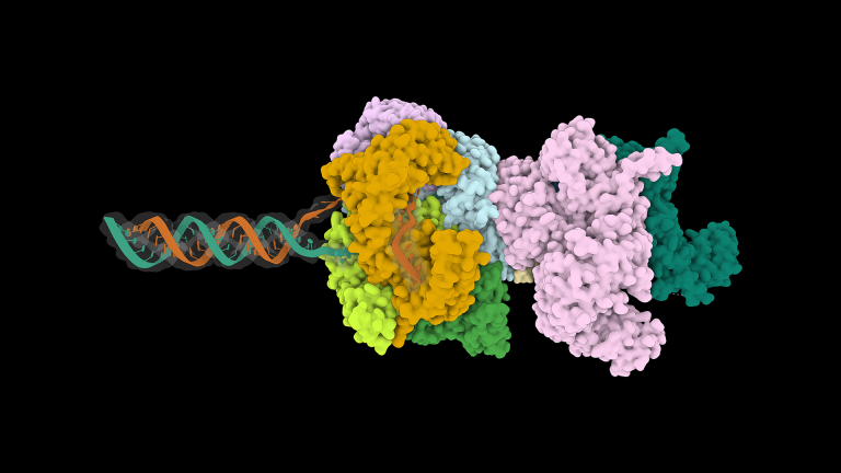
Other examples include basically every processor with HBM. HBM was founded as a way of step function increasing memory bandwidth above traditional forms of DRAM. It does this by operating with a much wider memory bus. These wide busses create issues related to IO counts, but HBM was designed from the ground up to be co-located within the same package. This subverts the IO issue while also allowing for much tighter integration.
A few more examples of 2.5D include Intel EMIB based products, Xilinx FPGA’s, AMD’s newest datacenter GPU, and Amazon Graviton 3.

3D packaging is taking an active die and packaging it on top of another active die. This was initially shipped with logic silicon at 55-micron pitches by Intel, but volume use cases will be at 36-micron and lower. TSMC and AMD will be shipping 3d stacked V-cache at a 17-micron pitch. This technology moves from bumps to through silicon vias (TSVs), and it has much more room to scale.
Other applications such as CMOS image sensors manufactured by Sony are already at 6.3-micron pitch. To keep the comparisons going, 36-micron pitch is 31x higher bump density, copper TSVs implemented at a 17-micron pitch would be 138x higher IO density, and CMOS image sensors by Sony are at 6.3-micron pitch are 567x higher IO density versus standard flip chip.

That was just a basic explanation of the major types of packaging, but we will delve deeper into the different types in this series. There are quite a few different bets companies have made on future packaging types, tools, and from which tool vendors. The equipment and IP side of things has a lot more excitement than people assume at first glance, but the basics need to be explained before we can delve deeper.
There are a lot of investable ideas and angles for this coming sea of innovation. Radical change is being driven by the slowdown of Moore’s Law. We are in the midst of the semiconductor design renaissance which is being pushed forward by advanced packaging.
Nothing behind the paywall in this article, but there will be more as we move into specific firms. As a reminder of what to expect, previous paywalls had us exclusively disclosing the packaging vendor for Graviton 3 (a certain blue company), and discussing process of record wins related to metal oxide photoresist and dry photoresist.